
White paper
Our semiconductor work focuses on the chip design, manufacturing and packaging innovations inside every connected device.
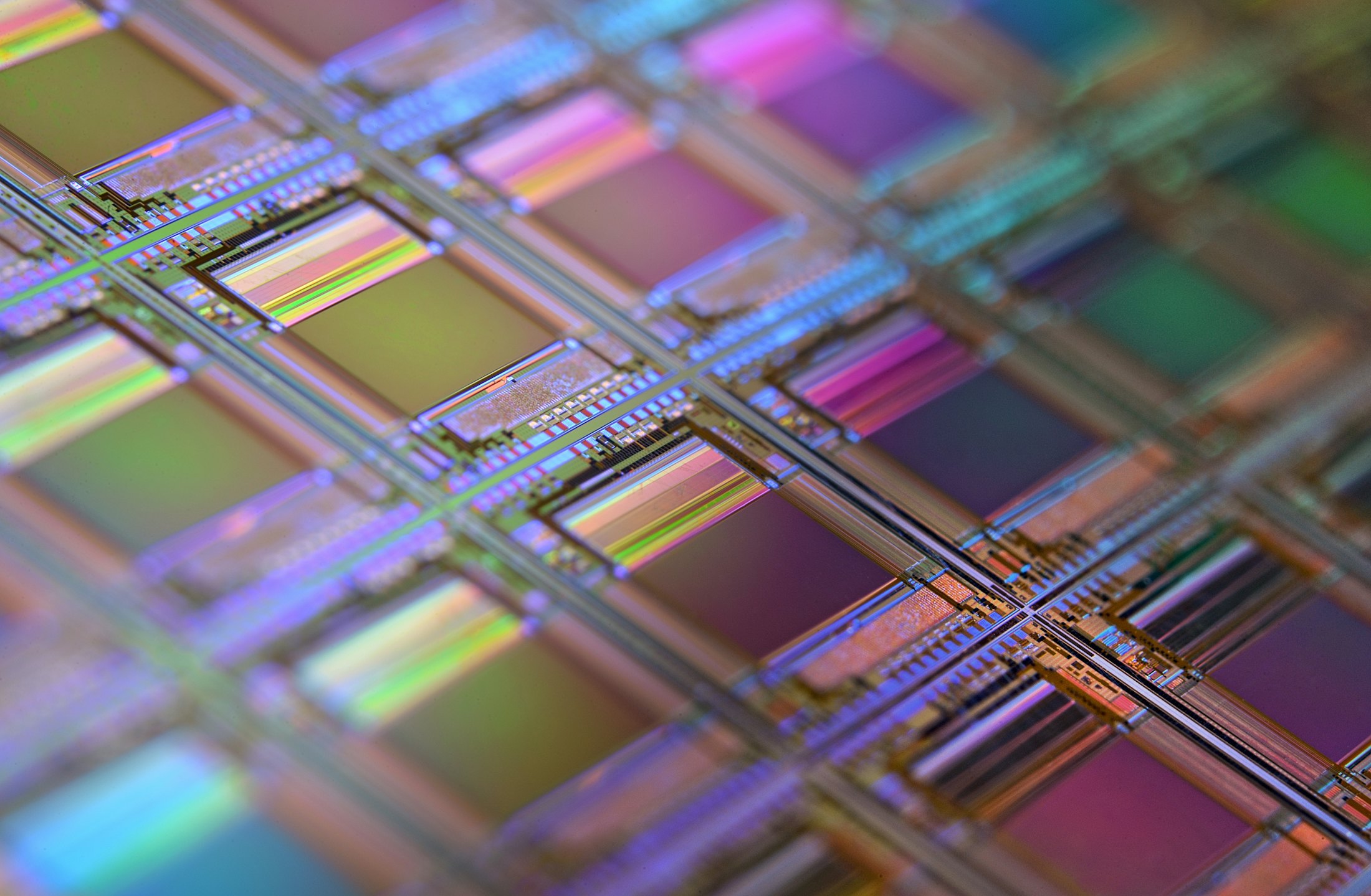
Every phone, car, data center and robot runs on semiconductors. As chips shrink, specialize and stack in new ways, inventions in design, manufacturing and packaging decide how fast, efficient and affordable technology can be. We follow innovation across the semiconductor value chain and make it available through fair licensing.
The semiconductor technologies we focus on sit inside nearly every electronic product. Here are a few of the ways they make a difference.
Advanced process technology that packs more transistors into less space.
Stacking and chiplet techniques that combine specialized dies in one package.
Low-power designs that extend battery life and cut data-center energy use.
Radio chips and filters that make 5G and Wi-Fi connections possible.
Sensors that capture sharper photos and help vehicles and robots see.
Chips that manage power for electric vehicles, chargers and renewable energy.
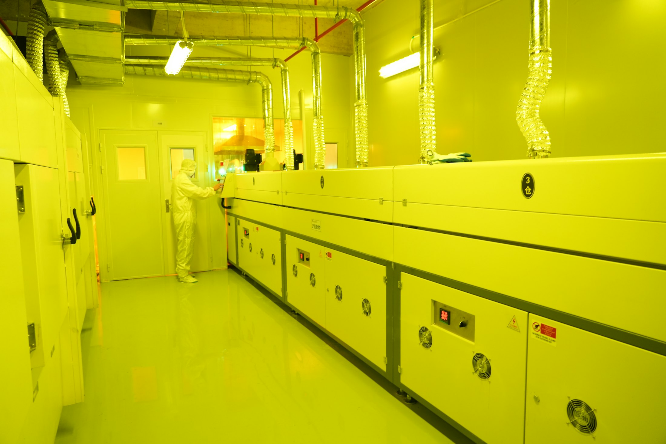
As shrinking transistors gets harder and more expensive, the industry is building upward instead. This paper explains how 3D stacking and chiplet packaging combine specialized dies into a single high-performance package, and what that means for phones, PCs and AI data centers.
Read moreLearn more about the research areas shaping semiconductors.
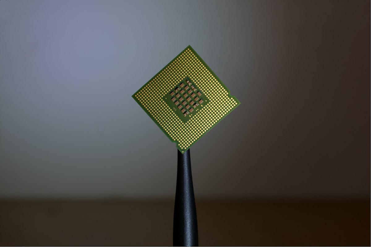
Chips power the digital world, and how they are designed and made affects energy use everywhere. Many of the semiconductor inventions we focus on help reduce that footprint:
Efficient semiconductors are better for device makers, for users and for the planet.
Our semiconductor work spans three connected areas.
We follow research across chip design, manufacturing and packaging.
We follow the interface and packaging standards that let chips work together.
We offer clear, fair licenses for the semiconductor technologies inside today’s products.
The semiconductor inventions we focus on are found in the interface and packaging standards used across the industry.
The semiconductor technologies we focus on sit inside nearly every electronic product.
Learn more